Electronics")
Panelization Guidelines For Odd-shaped PCB
As a PCB designer, we all know that several small PCBs can be grouped together for processing as a panel and PCB panelization is a method of designing an array of PCBs into a single processing piece for the PCB assemblers to improve production efficiency and lower manufacturing costs.
For the boards of regular shapes like rectangular boards, it is quite easy to design the PCB layout of the panel. When it comes to some odd-form boards, however, it is far more complicated to design the panel layout. So this guide is going to teach you how to handle with these troublesome PCBs to design optimal panel layout.
Panelization Methods
V-Groove Panelization Method: V-groove can only take a straight line and process square or rectangular PCBs. It can't process multiple boards at the same time or process odd shaped boards. There are strict precision requirements for V-groove depth. Generally speaking, this calls for cutting 1/3 the thickness of the board from the top and 1/3 the thickness from the bottom, collinear with the top cut, with a 30- to 45-degree circular cutting blade.
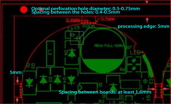
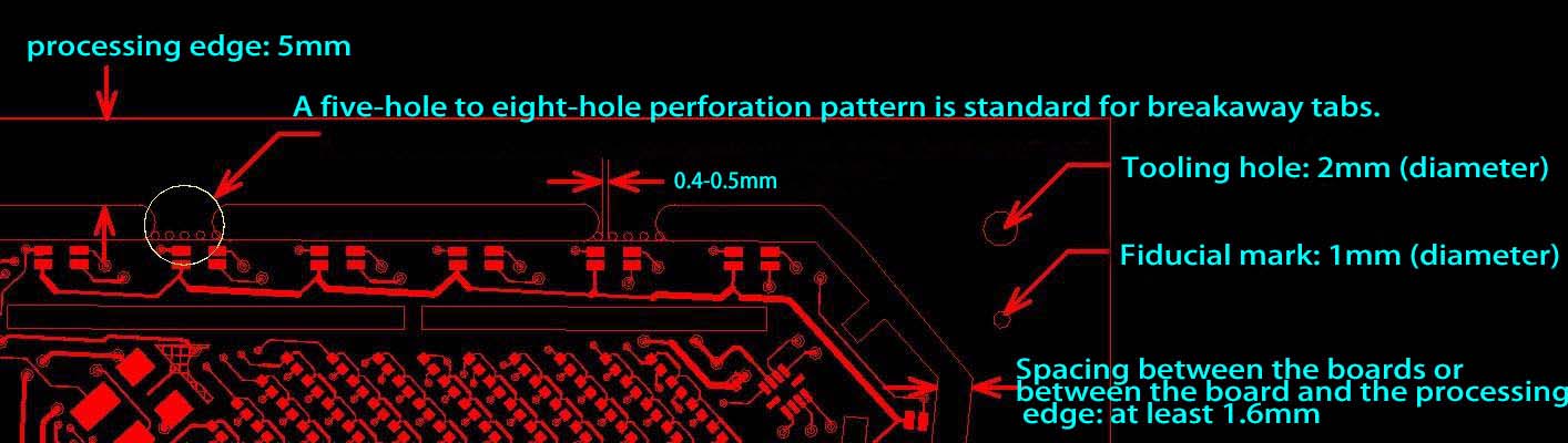
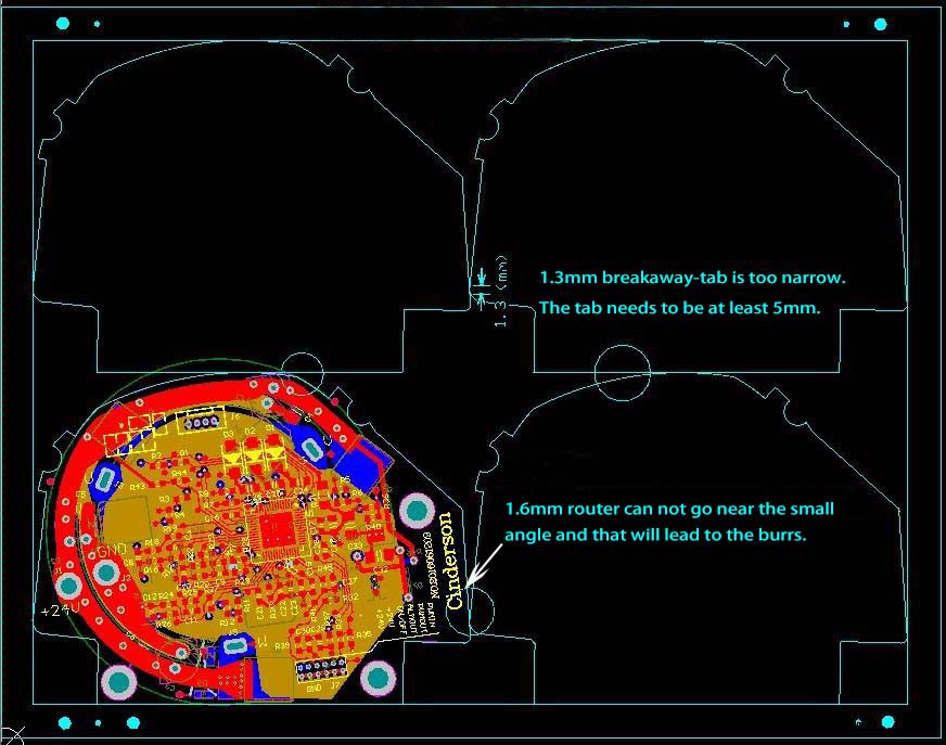
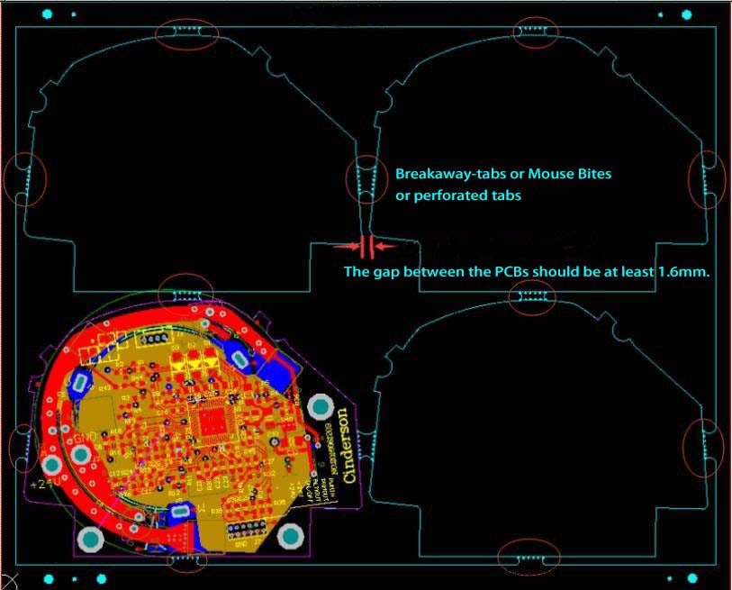
Breakaway-Tab Panelization Method: When V-grooves can’t be used, it is a good way to leave perforated tabs routing space between PCBs. For those odd-form PCBs, perforated-tab is needed to help connect the boards. The breakaway tab without perforations should be at least 3mm; while the perforated-tab should be at least 5mm. Generally, the perforated hole size is defined as follows:
Here we provide several odd-form PCB examples for you to better understand the panelization methods. Let’s get started.
Case No.1:
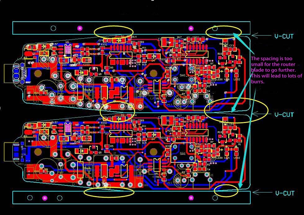
Bad Design
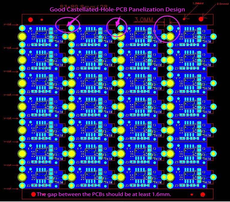
Good design
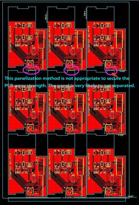
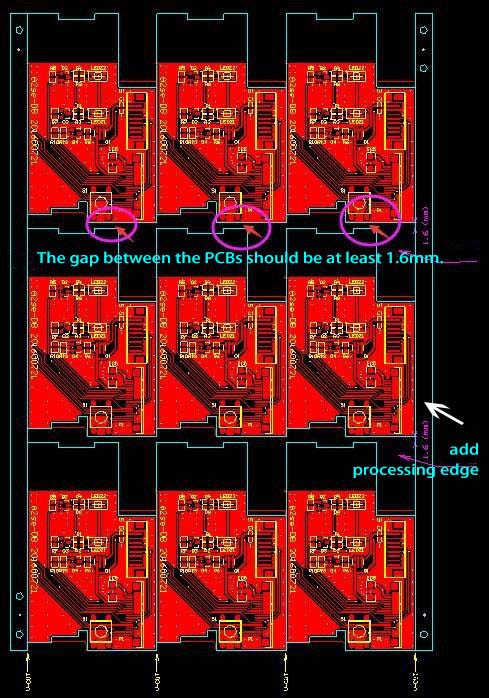
Case No.2:
Bad design
Good Design
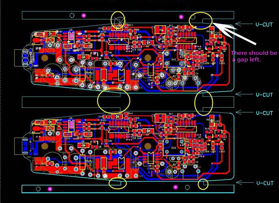
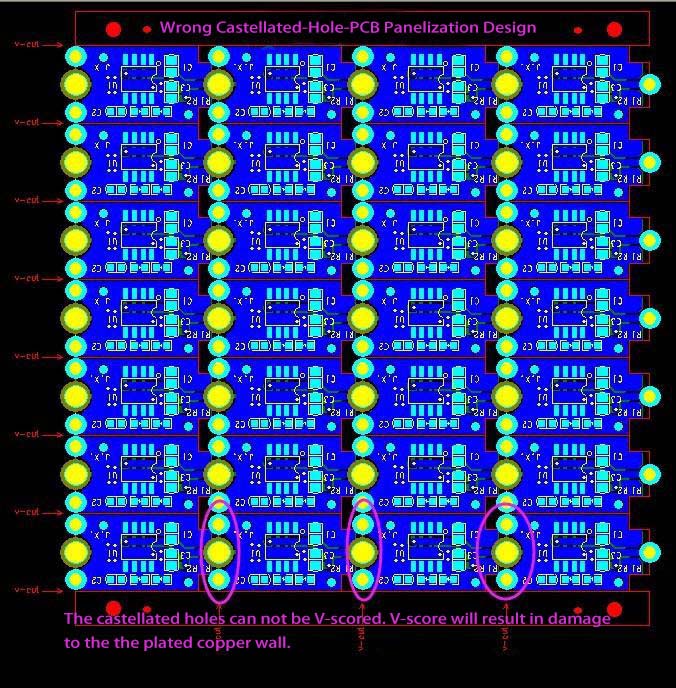
Case No.3:
Bad Design
Good Design
Case No.4:
Bad Design
Good Design