 Electronics")
Making a PCB - PCB Manufacture step by step
TinySine have provided PCB service in a long time. We specialise in providing prototype and small batch PCBs for designers, product development departments, niche market electronics companies, universities and research establishments. Many customers like our service. Here we introduce how we work.
Front-end tool data preparation
The board designer has prepared his layout on a Computer Aided Design or CAD system. Each CAD system uses its own internal data format, so the PCB industry has developed a standard output format to transfer the layout data to the manufacturer. This is Extended Gerber or RS274X. The Gerber files define the copper tracking layers (4 in the job we are following) as well as the soldermasks and component notations. Many designer like Eagle, This a guide of how to export gerber from Eagle.
Panel Cutting&Drilling the PCB
Drill the holes for leaded components and the via holes that link the copper layers together. First we use an X-ray drill to locate targets in the copper of the inner layers. The machine drills registration holes to ensure that we will drill precisely through the centre of the inner layer pads.
Electroless copper deposition
The first step in the plating process is the chemical deposition of a very thin layer of copper on the hole walls.
Image the outer layers.
We image the outer layers in a clean room to make sure that no dust gets onto the panel surface where it could cause a short or open circuit on the finished PCB.
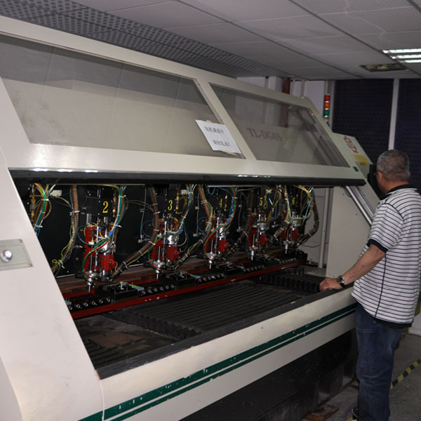
Plating
Next we electroplate the boards with copper. The operator loads the panels onto the flight bars. He checks all the clamps to ensure a good electrical connection.
Etch outer layers.
We have now plated the panel with 25 microns of copper through the hole and an additional 25 – 30 microns on the tracks and pads. The copper is covered with a thin layer of tin as an etch resist. Now we will remove the unwanted copper foil from the surface.
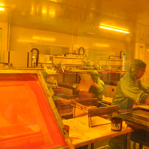
Apply soldermask.
Most boards have a epoxy-ink soldermask printed onto each side to protect the copper surface and prevent solder shorting between components during assembly.
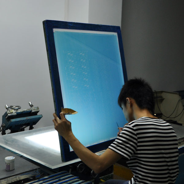
Silk-screen and cure.
Most PCBs have a component legend to show which component goes where. Today we use ink-jet printers to image the legends direct from the board digital data.
Worker are checking the silk
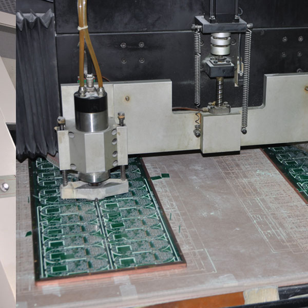
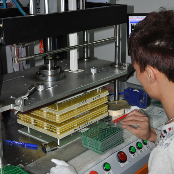
Profiling. -V-cut scoring
The final manufacturing stage is to profile the PCBs and cut them out of the production panel.
Alternatively we can profile the individual circuits on a V-cut or scoring machine. This has two cutters, one above and one below the panel. Each cuts a v-shaped groove about 1/3 of the thickness of the material, leaving a thin web holding the PCBs together...
Electrical test.
We electrically test every multilayer PCB against the original board data. Using a flying probe tester we check each net to ensure that it is complete (no open circuits) and does not short to any other net.
Final inspection.
In the last step of the process a team of sharp-eyed inspectors give each PCB a final careful check-over.